- Semiconductor Characterization: Analyze doping profiles in materials such as silicon, germanium, III-V compounds, and wide bandgap nitrides.
- Device Quality Control: Evaluate epitaxial layer uniformity, interface properties, and dopant distribution in MBE and MOCVD-grown structures.
- Impurity Profiling: Detect and quantify electrically active impurities that impact device performance.
- Advanced Device Development: Support the fabrication of solar cells, VCSELs, micro-LEDs, IR detectors, and quantum devices through precise material analysis.
ECVPro+
Advanced Electrochemical Capacitance Voltage
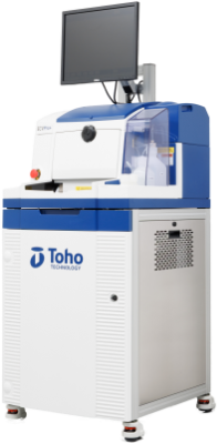
The Toho ECVPro+ is a market-leading, all-in-one system for carrier concentration profiling in semiconductor materials. Utilizing Electrochemical Capacitance Voltage (ECV) Profiling, it delivers unmatched accuracy and reliability in measuring dopant distribution across complex epitaxial structures. Designed for advanced semiconductor research and quality control, the ECVPro+ empowers users with deep insights into material behavior and device performance.
Applications
Most Advanced Measurement Capabilities
Advanced Features
- Built-in blast contact feature allowing for uniform oxide removal
- Dual-frequency and AC measurement modes for enhanced sensitivity
- Real-time etch visualization and interface analysis
Comprehensive Material Range
- III-V, II-VI, and IV semiconductors (e.g., GaAs, InP, GaN, SiC, ZnO, CdTe)
- Complex epitaxial structures and p-n junctions
- Nanomaterials, quantum dots, and IR sensors
Simplest Workflow
3-Step Operation
- Load Sample on vacuum stage
- Make Contact with probes
- Lock & Measure — automated recipe handles the rest
System Highlights
- Built-in blast contact (40V) ensures consistent Ohmic contact
- Platinum reference electrode eliminates manual calibration
- No need for mercury-based electrodes or manual adjustments
Superior Design
Camera & Optics
- Monochrome JAI GO-5101M-PMCL (5.1 MP, Visible + NIR)
- High sensitivity, sharpness, and low-light performance
- Adjustable contrast, gain, and exposure for accurate etch visualization
Fluid Handling System
- Vacuum-based manifold for electrolyte and DI water
- Chemically resistant tubing with leak-proof design
- Automatic fill, drain, and wash sequences
Cell Assembly & Sealing Rings
- Tool-free, 2-step sealing ring mounting
- Built-in counterweight for uniform pressure
- Optimized electrolyte circulation for consistent etching
Dynamic and Flexible Software
Recipe Automation
- Create and run complex etch profiles without supervision
- Pause to measure IV, CV, depletion profiles, or switch electrolytes
- Automated lamp intensity adjustment for consistent etch rates
ECVision Imaging
- Live visualization of etch progress and defect exposure
- Capture images at specific depths or junctions
- Integrated SPC tracking for process control
Reprocessing Software
- Adjust material valency, density, etch ring size, and correction factors
- Refine dopant concentration and depth resolution post-measurement
- Eliminate data corruption from electrolyte bubbles or disturbances
Unmatched Global Support
Global Presence
- 300+ systems installed worldwide
- Support centers in Chicago, San Jose, Paris, Tokyo, Shanghai, and more
- Applications labs in California, Japan, and China
Service & Reliability
- 90-day lead time, tariff-protected shipping from Japan
- Spare parts depots in the US, Japan, and China
- Compliant with NFPA-79, SEMI S2/S8/S14, CE
Applications
- Semiconductor Characterization: Analyze doping profiles in materials such as silicon, germanium, III-V compounds, and wide bandgap nitrides.
- Device Quality Control: Evaluate epitaxial layer uniformity, interface properties, and dopant distribution in MBE and MOCVD-grown structures.
- Impurity Profiling: Detect and quantify electrically active impurities that impact device performance.
- Advanced Device Development: Support the fabrication of solar cells, VCSELs, micro-LEDs, IR detectors, and quantum devices through precise material analysis.
Advanced Measurement Capabilities
The ECVPro+ sets a new standard in measurement precision. Its proprietary dual-frequency and AC measurement modes provide superior signal-to-noise ratios, enabling deeper and more accurate profiling of semiconductor layers. The system excels in characterizing p-n junctions, interface accumulation, and complex multi-layer structures. Pulsed etching technology ensures uniform material removal even in high-aluminum-content films, such as GaN and VCSELs, where traditional etching methods fall short. This capability is critical for researchers working with wide bandgap materials and high-performance optoelectronic devices.
Simplest Workflow
Designed with user efficiency in mind, the ECVPro+ simplifies the measurement process to just three steps: place the sample, lower the contacts, and close the door. From there, the system’s automated recipe engine takes over, executing precise etching and measurement sequences with minimal user intervention. Built-in features like the platinum reference electrode and blast contact function eliminate the need for manual calibration and reduce the risk of user error, making the system both accessible and reliable for routine and advanced users alike.
Superior Design
Every component of the ECVPro+ is engineered for performance and longevity. The system includes a high-resolution JAI camera (5.1 MP) with visible and NIR sensitivity, enabling real-time visualization of the etch process. The fluid handling system uses vacuum-driven manifolds to extend pump life and prevent leaks, while the modular cell assembly allows for easy maintenance and rapid sealing ring replacement. Available in both White Light and Ultraviolet configurations, the ECVPro+ supports a broad spectrum of materials, from standard III-V semiconductors to advanced nitrides and II-VI compounds.
Dynamic and Flexible Software
The ECVPro+ software suite offers unmatched flexibility and control. Users can create and automate complex measurement recipes, adjust lamp intensity dynamically, and monitor every step of the etch process in real time using the ECVision interface. The software also includes robust logging and diagnostic tools, enabling users to trace measurement history, identify anomalies, and refine results post-measurement using the built-in reprocessing engine. Whether you’re probing nanomaterials, quantum dots, or bulk substrates, the software adapts to your needs with precision and ease.
Unmatched Global Support
With over 300 systems deployed worldwide, the ECVPro+ is trusted by leading research institutions and semiconductor manufacturers across North America, Europe, and Asia. Toho’s global support network includes regional service centers in Chicago, San Jose, Paris, Shanghai, and more, ensuring rapid response times and expert assistance wherever you are. Spare parts depots in the U.S., Japan, and China further reduce downtime, while Toho’s legacy of Japanese engineering excellence—dating back to 1829—guarantees quality and reliability in every system.