- Semiconductor Characterization: Analyze doping profiles in materials such as silicon, germanium, III-V compounds, and wide bandgap nitrides.
- Device Quality Control: Evaluate epitaxial layer uniformity, interface properties, and dopant distribution in MBE and MOCVD-grown structures.
- Impurity Profiling: Detect and quantify electrically active impurities that impact device performance.
- Advanced Device Development: Support the fabrication of solar cells, VCSELs, micro-LEDs, IR detectors, and quantum devices through precise material analysis.
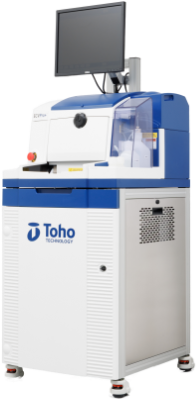
ECVPro+
Advanced Electrochemical Capacitance Voltage
The Toho ECVPro+ is a market-leading, all-in-one system for carrier concentration profiling in semiconductor materials. Utilizing Electrochemical Capacitance Voltage (ECV) Profiling, it delivers unmatched accuracy and reliability in measuring dopant distribution across complex epitaxial structures. Designed for advanced semiconductor research and quality control, the ECVPro+ empowers users with deep insights into material behavior and device performance.
Applications
Most Advanced Measurement Capabilities
Advanced Features
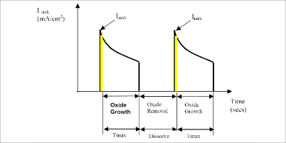
- Built-in blast contact feature allowing for uniform oxide removal
- Dual-frequency and AC measurement modes for enhanced sensitivity
- Real-time etch visualization and interface analysis
Comprehensive Material Range
- III-V, II-VI, and IV semiconductors (e.g., GaAs, InP, GaN, SiC, ZnO, CdTe)
- Complex epitaxial structures and p-n junctions
- Nanomaterials, quantum dots, and IR sensors
Simplest Workflow
3-Step Operation
- Load Sample on vacuum stage
- Make Contact with probes
- Lock & Measure — automated recipe handles the rest
System Highlights
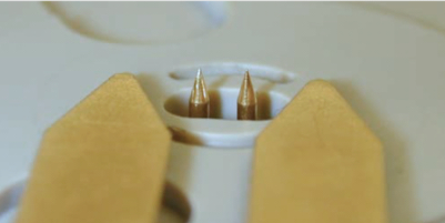
- Built-in blast contact (40V) ensures consistent Ohmic contact
- Platinum reference electrode eliminates manual calibration
- No need for mercury-based electrodes or manual adjustments
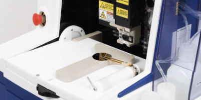
Superior Design
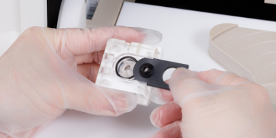
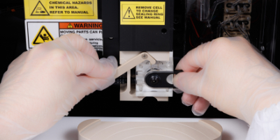
Cell Assembly & Sealing Rings
- Tool-free, 2-step sealing ring mounting
- Built-in counterweight for uniform pressure
- Optimized electrolyte circulation for consistent etching
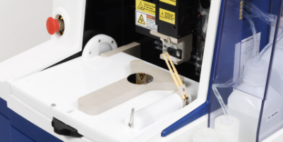
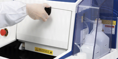
Fluid Handling System
- Vacuum-based manifold for electrolyte and DI water
- Chemically resistant tubing with leak-proof design
- Automatic fill, drain, and wash sequences
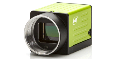
Camera & Optics
- Monochrome JAI GO-5101M-PMCL (5.1 MP, Visible + NIR)
- High sensitivity, sharpness, and low-light performance
- Adjustable contrast, gain, and exposure for accurate etch visualization
Dynamic and Flexible Software
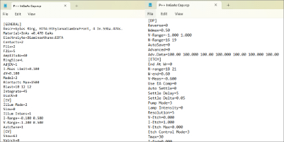
Recipe Automation
- Create and run complex etch profiles without supervision
- Pause to measure IV, CV, depletion profiles, or switch electrolytes
- Automated lamp intensity adjustment for consistent etch rates
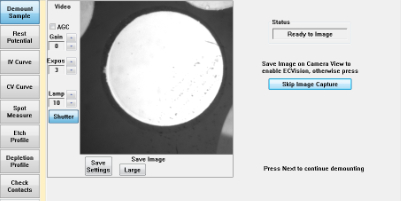
ECVision* Imaging
- Live visualization of etch progress and defect exposure
- Capture images at specific depths or junctions
- Integrated SPC tracking for process control
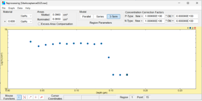
Reprocessing Software
- Adjust material valency, density, etch ring size, and correction factors
- Refine dopant concentration and depth resolution post-measurement
- Eliminate data corruption from electrolyte bubbles or disturbances
* ECVision is enabled by optimum surface reflection. Textured or patterned sample surfaces impact reflectivity and impair visibility of De-bubbling and in-situ etching quality and, in some cases, the accuracy of carrier concentration measurements at various depths.
Unmatched Global Support
Global Presence
- 300+ systems installed worldwide
- Support centers in Chicago, San Jose, Paris, Tokyo, Shanghai, and more
- Applications labs in California, Japan, and China
Service & Reliability
- 90-day lead time, tariff-protected shipping from Japan
- Spare parts depots in the US, Japan, and China
- Compliant with NFPA-79, SEMI S2/S8/S14, CE